制服欧美另类中文字幕第三页_欧美三级经典国产一区_日本日本妇人成熟免费2020_午夜视频福利久久_制服丝袜激情视频_动漫巨乳美女抖奶30网站_抖阴富二代下载_国产精品456在线播放_中文字幕波多野结衣av一区二区_日韩av高清亚洲无码痴汉色色


400-9988-118
中文|English


SURAGUS EddyCus? TF map 2530


Eddy-Cus TF map 2530


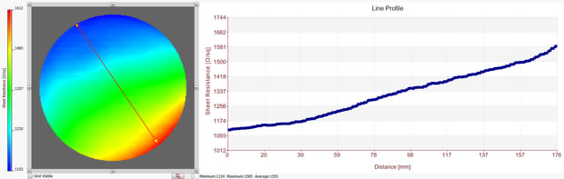
EddyCus? TF map 2530 Series – Non-contact Sheet Resistance and Metal Layer Thickness Mapping Device

The Eddy-Cus? TF map 2530 Series auto-mat-ic-ally meas-ures the sheet res-ist-ance of large samples up to 300 x 300 mm2 (12 x 12 inches) in non-con-tact mode. Upon manu-al sample po-s-i-tion-ing the device auto-mat-ic-ally meas-ures and dis-plays an ac-cur-ate map-ping of the sheet res-ist-ance across the en-tire sample area. The meas-ure-ment set-tings al-low eas-ily and flex-ibly to choose between fast meas-ure-ment times of be-low 1 minute or high spa-tial meas-ure-ment res-ol-u-tion of more than 100,000 meas-ure-ment points.

Highlights

· Non-contact
· Fast and precise measurement
· High resolution mapping of conductive thin films
· Imaging of substrates up to 300 x 300 mm (12 x 12 inches)
· Characterization even of hidden and encapsulated conductive layers
· Various software-integrated analysis functions (e.g. sheet resistance distribution, line scans, single point analysis)
· Measurement data saving and export functions
· Defect detection and coating analysis

Characteristics

· Technology: non-contact eddy current
· Imaging by multipoint mapping
· Positioning area: 300 mm x 300 mm
· Sampling area: 300 x 300 mm
· Recommended sample sizes: 1 inch to 12 inch or 25 to 300 mm

Applications

Coated architectural glass, e.g. LowE
Displays, touch screens and flat panel displays
OLED and LED applications
Smart glass
Graphene layers
Photovoltaic wafers and cells
Semiconductor wafers
Metallization layers and wafer metallization
De-icing and heating applications
Battery electrodes
Conductively coated paper and conductive textiles